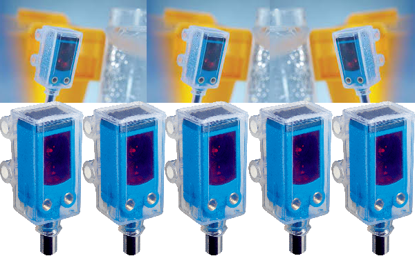
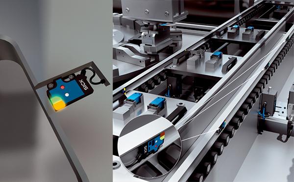
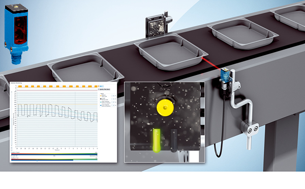
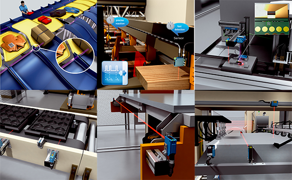
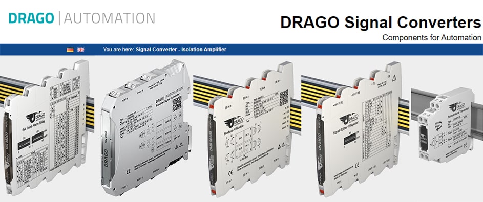
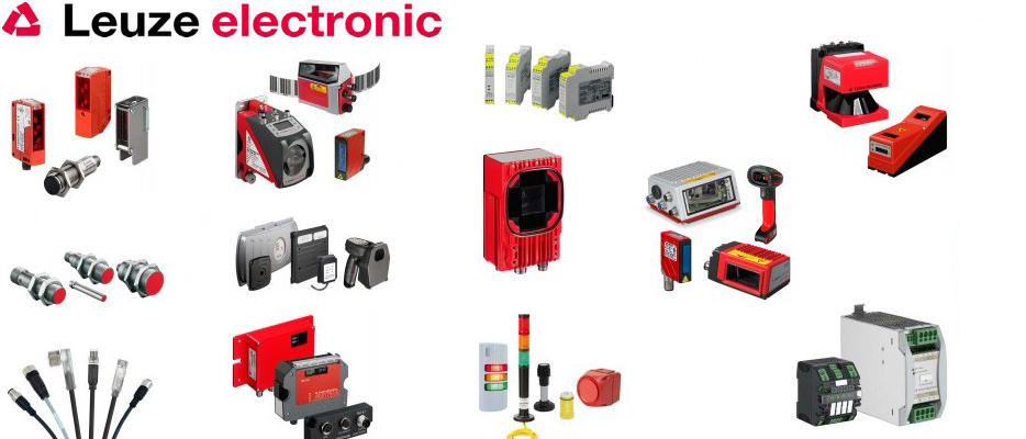
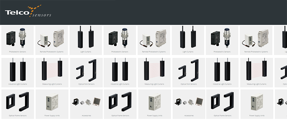
Cảm biến phát hiện các đối tượng và đo chiều rộng, độ dày và các kích thước khác của chúng, với phương pháp quét CCD hoặc laser để đáp ứng các nhu cầu ứng dụng và độ chính xác khác nhau.
A charge-coupled device (CCD) is an integrated circuit containing an array of linked, or coupled, capacitors. Under the control of an external circuit, each capacitor can transfer its electric charge to a neighboring capacitor. CCD sensors are a major technology used in digital imaging.
In a CCD image sensor, pixels are represented by p-doped metal–oxide–semiconductor (MOS) capacitors. These MOS capacitors, the basic building blocks of a CCD,[1] are biased above the threshold for inversion when image acquisition begins, allowing the conversion of incoming photons into electron charges at the semiconductor-oxide interface; the CCD is then used to read out these charges. Although CCDs are not the only technology to allow for light detection, CCD image sensors are widely used in professional, medical, and scientific applications where high-quality image data are required. In applications with less exacting quality demands, such as consumer and professional digital cameras, active pixel sensors, also known as CMOS sensors (complementary MOS sensors), are generally used. However, the large quality advantage CCDs enjoyed early on has narrowed over time and since the late 2010s CMOS sensors are the dominant technology, having largely if not completely replaced CCD image sensors.
Basics of operation
 The charge packets (electrons, blue) are collected in potential wells (yellow) created by applying positive voltage at the gate electrodes (G). Applying positive voltage to the gate electrode in the correct sequence transfers the charge packets.

In a CCD for capturing images, there is a photoactive region (an epitaxial layer of silicon), and a transmission region made out of a shift register (the CCD, properly speaking).
An image is projected through a lens onto the capacitor array (the photoactive region), causing each capacitor to accumulate an electric charge proportional to the light intensity at that location. A one-dimensional array, used in line-scan cameras, captures a single slice of the image, whereas a two-dimensional array, used in video and still cameras, captures a two-dimensional picture corresponding to the scene projected onto the focal plane of the sensor. Once the array has been exposed to the image, a control circuit causes each capacitor to transfer its contents to its neighbor (operating as a shift register). The last capacitor in the array dumps its charge into a charge amplifier, which converts the charge into a voltage. By repeating this process, the controlling circuit converts the entire contents of the array in the semiconductor to a sequence of voltages. In a digital device, these voltages are then sampled, digitized, and usually stored in memory; in an analog device (such as an analog video camera), they are processed into a continuous analog signal (e.g. by feeding the output of the charge amplifier into a low-pass filter), which is then processed and fed out to other circuits for transmission, recording, or other processing.
Detailed physics of operation
Charge generation
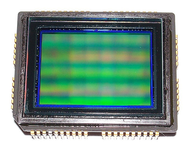 Sony ICX493AQA 10.14-megapixel APS-C (23.4 × 15.6 mm) CCD from digital camera Sony α DSLR-A200 or DSLR-A300, sensor side
Before the MOS capacitors are exposed to light, they are biased into the depletion region; in n-channel CCDs, the silicon under the bias gate is slightly p-doped or intrinsic. The gate is then biased at a positive potential, above the threshold for strong inversion, which will eventually result in the creation of an n channel below the gate as in a MOSFET. However, it takes time to reach this thermal equilibrium: up to hours in high-end scientific cameras cooled at low temperature. Initially after biasing, the holes are pushed far into the substrate, and no mobile electrons are at or near the surface; the CCD thus operates in a non-equilibrium state called deep depletion. Then, when electron–hole pairs are generated in the depletion region, they are separated by the electric field, the electrons move toward the surface, and the holes move toward the substrate. Four pair-generation processes can be identified:
- photo-generation (up to 95% of quantum efficiency),
- generation in the depletion region,
- generation at the surface, and
- generation in the neutral bulk.
The last three processes are known as dark-current generation, and add noise to the image; they can limit the total usable integration time. The accumulation of electrons at or near the surface can proceed either until image integration is over and charge begins to be transferred, or thermal equilibrium is reached. In this case, the well is said to be full. The maximum capacity of each well is known as the well depth, typically about 105 electrons per pixel.
Design and manufacturing
The photoactive region of a CCD is, generally, an epitaxial layer of silicon. It is lightly p doped (usually with boron) and is grown upon a substrate material, often p++. In buried-channel devices, the type of design utilized in most modern CCDs, certain areas of the surface of the silicon are ion implanted with phosphorus, giving them an n-doped designation. This region defines the channel in which the photogenerated charge packets will travel. Simon Sze details the advantages of a buried-channel device:
This thin layer (= 0.2–0.3 micron) is fully depleted and the accumulated photogenerated charge is kept away from the surface. This structure has the advantages of higher transfer efficiency and lower dark current, from reduced surface recombination. The penalty is smaller charge capacity, by a factor of 2–3 compared to the surface-channel CCD.
The gate oxide, i.e. the capacitor dielectric, is grown on top of the epitaxial layer and substrate.
Later in the process, polysilicon gates are deposited by chemical vapor deposition, patterned with photolithography, and etched in such a way that the separately phased gates lie perpendicular to the channels. The channels are further defined by utilization of the LOCOS process to produce the channel stop region.
Channel stops are thermally grown oxides that serve to isolate the charge packets in one column from those in another. These channel stops are produced before the polysilicon gates are, as the LOCOS process utilizes a high-temperature step that would destroy the gate material. The channel stops are parallel to, and exclusive of, the channel, or "charge carrying", regions.
Channel stops often have a p+ doped region underlying them, providing a further barrier to the electrons in the charge packets (this discussion of the physics of CCD devices assumes an electron transfer device, though hole transfer is possible).
The clocking of the gates, alternately high and low, will forward and reverse bias the diode that is provided by the buried channel (n-doped) and the epitaxial layer (p-doped). This will cause the CCD to deplete, near the p–n junction and will collect and move the charge packets beneath the gates—and within the channels—of the device.
CCD manufacturing and operation can be optimized for different uses. The above process describes a frame transfer CCD. While CCDs may be manufactured on a heavily doped p++ wafer it is also possible to manufacture a device inside p-wells that have been placed on an n-wafer. This second method, reportedly, reduces smear, dark current, and infrared and red response. This method of manufacture is used in the construction of interline-transfer devices.
Another version of CCD is called a peristaltic CCD. In a peristaltic charge-coupled device, the charge-packet transfer operation is analogous to the peristaltic contraction and dilation of the digestive system. The peristaltic CCD has an additional implant that keeps the charge away from the silicon/silicon dioxide interface and generates a large lateral electric field from one gate to the next. This provides an additional driving force to aid in transfer of the charge packets.
Architecture
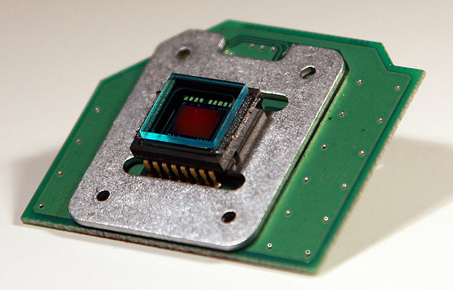 CCD from a 2.1-megapixel Argus digital camera
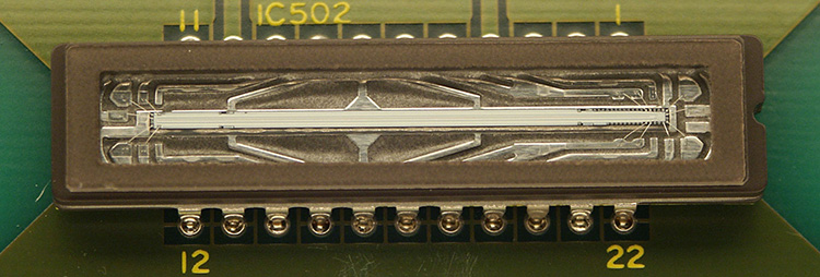 One-dimensional CCD image sensor from a fax machine
The CCD image sensors can be implemented in several different architectures. The most common are full-frame, frame-transfer, and interline. The distinguishing characteristic of each of these architectures is their approach to the problem of shuttering.
In a full-frame device, all of the image area is active, and there is no electronic shutter. A mechanical shutter must be added to this type of sensor or the image smears as the device is clocked or read out.
With a frame-transfer CCD, half of the silicon area is covered by an opaque mask (typically aluminum). The image can be quickly transferred from the image area to the opaque area or storage region with acceptable smear of a few percent. That image can then be read out slowly from the storage region while a new image is integrating or exposing in the active area. Frame-transfer devices typically do not require a mechanical shutter and were a common architecture for early solid-state broadcast cameras. The downside to the frame-transfer architecture is that it requires twice the silicon real estate of an equivalent full-frame device; hence, it costs roughly twice as much.
The interline architecture extends this concept one step further and masks every other column of the image sensor for storage. In this device, only one pixel shift has to occur to transfer from image area to storage area; thus, shutter times can be less than a microsecond and smear is essentially eliminated. The advantage is not free, however, as the imaging area is now covered by opaque strips dropping the fill factor to approximately 50 percent and the effective quantum efficiency by an equivalent amount. Modern designs have addressed this deleterious characteristic by adding microlenses on the surface of the device to direct light away from the opaque regions and on the active area. Microlenses can bring the fill factor back up to 90 percent or more depending on pixel size and the overall system's optical design.
The choice of architecture comes down to one of utility. If the application cannot tolerate an expensive, failure-prone, power-intensive mechanical shutter, an interline device is the right choice. Consumer snap-shot cameras have used interline devices. On the other hand, for those applications that require the best possible light collection and issues of money, power and time are less important, the full-frame device is the right choice. Astronomers tend to prefer full-frame devices. The frame-transfer falls in between and was a common choice before the fill-factor issue of interline devices was addressed. Today, frame-transfer is usually chosen when an interline architecture is not available, such as in a back-illuminated device.
CCDs containing grids of pixels are used in digital cameras, optical scanners, and video cameras as light-sensing devices. They commonly respond to 70 percent of the incident light (meaning a quantum efficiency of about 70 percent) making them far more efficient than photographic film, which captures only about 2 percent of the incident light.
Most common types of CCDs are sensitive to near-infrared light, which allows infrared photography, night-vision devices, and zero lux (or near zero lux) video-recording/photography. For normal silicon-based detectors, the sensitivity is limited to 1.1 μm. One other consequence of their sensitivity to infrared is that infrared from remote controls often appears on CCD-based digital cameras or camcorders if they do not have infrared blockers.
Cooling reduces the array's dark current, improving the sensitivity of the CCD to low light intensities, even for ultraviolet and visible wavelengths. Professional observatories often cool their detectors with liquid nitrogen to reduce the dark current, and therefore the thermal noise, to negligible levels.
Frame transfer CCD
 A frame transfer CCD sensor
The frame transfer CCD imager was the first imaging structure proposed for CCD Imaging by Michael Tompsett at Bell Laboratories. A frame transfer CCD is a specialized CCD, often used in astronomy and some professional video cameras, designed for high exposure efficiency and correctness.
The normal functioning of a CCD, astronomical or otherwise, can be divided into two phases: exposure and readout. During the first phase, the CCD passively collects incoming photons, storing electrons in its cells. After the exposure time is passed, the cells are read out one line at a time. During the readout phase, cells are shifted down the entire area of the CCD. While they are shifted, they continue to collect light. Thus, if the shifting is not fast enough, errors can result from light that falls on a cell holding charge during the transfer. These errors are referred to as "vertical smear" and cause a strong light source to create a vertical line above and below its exact location. In addition, the CCD cannot be used to collect light while it is being read out. Unfortunately, a faster shifting requires a faster readout, and a faster readout can introduce errors in the cell charge measurement, leading to a higher noise level.
A frame transfer CCD solves both problems: it has a shielded, not light sensitive, area containing as many cells as the area exposed to light. Typically, this area is covered by a reflective material such as aluminium. When the exposure time is up, the cells are transferred very rapidly to the hidden area. Here, safe from any incoming light, cells can be read out at any speed one deems necessary to correctly measure the cells' charge. At the same time, the exposed part of the CCD is collecting light again, so no delay occurs between successive exposures.
The disadvantage of such a CCD is the higher cost: the cell area is basically doubled, and more complex control electronics are needed.
Intensified charge-coupled device
An intensified charge-coupled device (ICCD) is a CCD that is optically connected to an image intensifier that is mounted in front of the CCD.
An image intensifier includes three functional elements: a photocathode, a micro-channel plate (MCP) and a phosphor screen. These three elements are mounted one close behind the other in the mentioned sequence. The photons which are coming from the light source fall onto the photocathode, thereby generating photoelectrons. The photoelectrons are accelerated towards the MCP by an electrical control voltage, applied between photocathode and MCP. The electrons are multiplied inside of the MCP and thereafter accelerated towards the phosphor screen. The phosphor screen finally converts the multiplied electrons back to photons which are guided to the CCD by a fiber optic or a lens.
An image intensifier inherently includes a shutter functionality: If the control voltage between the photocathode and the MCP is reversed, the emitted photoelectrons are not accelerated towards the MCP but return to the photocathode. Thus, no electrons are multiplied and emitted by the MCP, no electrons are going to the phosphor screen and no light is emitted from the image intensifier. In this case no light falls onto the CCD, which means that the shutter is closed. The process of reversing the control voltage at the photocathode is called gating and therefore ICCDs are also called gateable CCD cameras.
Besides the extremely high sensitivity of ICCD cameras, which enable single photon detection, the gateability is one of the major advantages of the ICCD over the EMCCD cameras. The highest performing ICCD cameras enable shutter times as short as 200 picoseconds.
ICCD cameras are in general somewhat higher in price than EMCCD cameras because they need the expensive image intensifier. On the other hand, EMCCD cameras need a cooling system to cool the EMCCD chip down to temperatures around 170 K (−103 °C). This cooling system adds additional costs to the EMCCD camera and often yields heavy condensation problems in the application.
ICCDs are used in night vision devices and in various scientific applications.
Electron-multiplying CCD
 Electrons are transferred serially through the gain stages making up the multiplication register of an EMCCD. The high voltages used in these serial transfers induce the creation of additional charge carriers through impact ionisation.
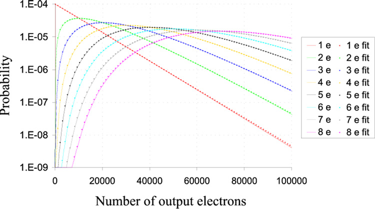 in an EMCCD there is a dispersion (variation) in the number of electrons output by the multiplication register for a given (fixed) number of input electrons (shown in the legend on the right). The probability distribution for the number of output electrons is plotted logarithmically on the vertical axis for a simulation of a multiplication register. Also shown are results from the empirical fit equation shown on this page.
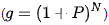
An electron-multiplying CCD (EMCCD, also known as an L3Vision CCD, a product commercialized by e2v Ltd., GB, L3CCD or Impactron CCD, a now-discontinued product offered in the past by Texas Instruments) is a charge-coupled device in which a gain register is placed between the shift register and the output amplifier. The gain register is split up into a large number of stages. In each stage, the electrons are multiplied by impact ionization in a similar way to an avalanche diode. The gain probability at every stage of the register is small (P < 2%), but as the number of elements is large (N > 500), the overall gain can be very high
, with single input electrons giving many thousands of output electrons. Reading a signal from a CCD gives a noise background, typically a few electrons. In an EMCCD, this noise is superimposed on many thousands of electrons rather than a single electron; the devices' primary advantage is thus their negligible readout noise. The use of avalanche breakdown for amplification of photo charges had already been described in the U.S. Patent 3,761,744 in 1973 by George E. Smith/Bell Telephone Laboratories.
EMCCDs show a similar sensitivity to intensified CCDs (ICCDs). However, as with ICCDs, the gain that is applied in the gain register is stochastic and the exact gain that has been applied to a pixel's charge is impossible to know. At high gains (> 30), this uncertainty has the same effect on the signal-to-noise ratio (SNR) as halving the quantum efficiency (QE) with respect to operation with a gain of unity. However, at very low light levels (where the quantum efficiency is most important), it can be assumed that a pixel either contains an electron—or not. This removes the noise associated with the stochastic multiplication at the risk of counting multiple electrons in the same pixel as a single electron. To avoid multiple counts in one pixel due to coincident photons in this mode of operation, high frame rates are essential. The dispersion in the gain is shown in the graph on the right. For multiplication registers with many elements and large gains it is well modelled by the equation:
where P is the probability of getting n output electrons given m input electrons and a total mean multiplication register gain of g.Because of the lower costs and better resolution, EMCCDs are capable of replacing ICCDs in many applications. ICCDs still have the advantage that they can be gated very fast and thus are useful in applications like range-gated imaging. EMCCD cameras indispensably need a cooling system—using either thermoelectric cooling or liquid nitrogen—to cool the chip down to temperatures in the range of −65 to −95 °C (−85 to −139 °F). This cooling system unfortunately adds additional costs to the EMCCD imaging system and may yield condensation problems in the application. However, high-end EMCCD cameras are equipped with a permanent hermetic vacuum system confining the chip to avoid condensation issues.
The low-light capabilities of EMCCDs find use in astronomy and biomedical research, among other fields. In particular, their low noise at high readout speeds makes them very useful for a variety of astronomical applications involving low light sources and transient events such as lucky imaging of faint stars, high speed photon counting photometry, Fabry-Pérot spectroscopy and high-resolution spectroscopy. More recently, these types of CCDs have broken into the field of biomedical research in low-light applications including small animal imaging, single-molecule imaging, Raman spectroscopy, super resolution microscopy as well as a wide variety of modern fluorescence microscopy techniques thanks to greater SNR in low-light conditions in comparison with traditional CCDs and ICCDs.
In terms of noise, commercial EMCCD cameras typically have clock-induced charge (CIC) and dark current (dependent on the extent of cooling) that together lead to an effective readout noise ranging from 0.01 to 1 electrons per pixel read. However, recent improvements in EMCCD technology have led to a new generation of cameras capable of producing significantly less CIC, higher charge transfer efficiency and an EM gain 5 times higher than what was previously available. These advances in low-light detection lead to an effective total background noise of 0.001 electrons per pixel read, a noise floor unmatched by any other low-light imaging device.
Use in astronomy
 Array of 30 CCDs used on the Sloan Digital Sky Survey telescope imaging camera, an example of "drift-scanning".
Due to the high quantum efficiencies of charge-coupled device (CCD) (the ideal quantum efficiency is 100%, one generated electron per incident photon), linearity of their outputs, ease of use compared to photographic plates, and a variety of other reasons, CCDs were very rapidly adopted by astronomers for nearly all UV-to-infrared applications.
Thermal noise and cosmic rays may alter the pixels in the CCD array. To counter such effects, astronomers take several exposures with the CCD shutter closed and opened. The average of images taken with the shutter closed is necessary to lower the random noise. Once developed, the dark frame average image is then subtracted from the open-shutter image to remove the dark current and other systematic defects (dead pixels, hot pixels, etc.) in the CCD. Newer Skipper CCDs counter noise by collecting data with the same collected charge multiple times and has applications in precision light Dark Matter searches and neutrino measurements.
The Hubble Space Telescope, in particular, has a highly developed series of steps (“data reduction pipeline”) to convert the raw CCD data to useful images.
CCD cameras used in astrophotography often require sturdy mounts to cope with vibrations from wind and other sources, along with the tremendous weight of most imaging platforms. To take long exposures of galaxies and nebulae, many astronomers use a technique known as auto-guiding. Most autoguiders use a second CCD chip to monitor deviations during imaging. This chip can rapidly detect errors in tracking and command the mount motors to correct for them.
An unusual astronomical application of CCDs, called drift-scanning, uses a CCD to make a fixed telescope behave like a tracking telescope and follow the motion of the sky. The charges in the CCD are transferred and read in a direction parallel to the motion of the sky, and at the same speed. In this way, the telescope can image a larger region of the sky than its normal field of view. The Sloan Digital Sky Survey is the most famous example of this, using the technique to produce a survey of over a quarter of the sky.
In addition to imagers, CCDs are also used in an array of analytical instrumentation including spectrometers and interferometers.
Color cameras
 A Bayer filter on a CCD
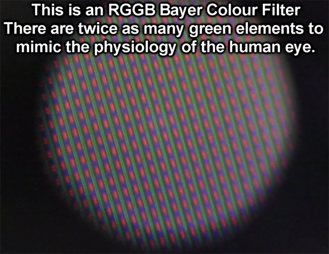 x80 microscope view of an RGGB Bayer filter on a 240 line Sony CCD PAL Camcorder CCD sensor
Digital color cameras generally use a Bayer mask over the CCD. Each square of four pixels has one filtered red, one blue, and two green (the human eye is more sensitive to green than either red or blue). The result of this is that luminance information is collected at every pixel, but the color resolution is lower than the luminance resolution.
Better color separation can be reached by three-CCD devices (3CCD) and a dichroic beam splitter prism, that splits the image into red, green and blue components. Each of the three CCDs is arranged to respond to a particular color. Many professional video camcorders, and some semi-professional camcorders, use this technique, although developments in competing CMOS technology have made CMOS sensors, both with beam-splitters and bayer filters, increasingly popular in high-end video and digital cinema cameras. Another advantage of 3CCD over a Bayer mask device is higher quantum efficiency (higher light sensitivity), because most of the light from the lens enters one of the silicon sensors, while a Bayer mask absorbs a high proportion (more than 2/3) of the light falling on each pixel location.
For still scenes, for instance in microscopy, the resolution of a Bayer mask device can be enhanced by microscanning technology. During the process of color co-site sampling, several frames of the scene are produced. Between acquisitions, the sensor is moved in pixel dimensions, so that each point in the visual field is acquired consecutively by elements of the mask that are sensitive to the red, green, and blue components of its color. Eventually every pixel in the image has been scanned at least once in each color and the resolution of the three channels become equivalent (the resolutions of red and blue channels are quadrupled while the green channel is doubled).
Sensor sizes
Sensors (CCD / CMOS) come in various sizes, or image sensor formats. These sizes are often referred to with an inch fraction designation such as 1/1.8″ or 2/3″ called the optical format. This measurement originates back in the 1950s and the time of Vidicon tubes.
Blooming
 Vertical smear
When a CCD exposure is long enough, eventually the electrons that collect in the "bins" in the brightest part of the image will overflow the bin, resulting in blooming. The structure of the CCD allows the electrons to flow more easily in one direction than another, resulting in vertical streaking.
Some anti-blooming features that can be built into a CCD reduce its sensitivity to light by using some of the pixel area for a drain structure. James M. Early developed a vertical anti-blooming drain that would not detract from the light collection area, and so did not reduce light sensitivity.
(DienElectric.com lược dịch theo Wikipedia)


 dienelectrics@gmail.com
 0909186879